Which GPU Computes Which Format: Ampere to Rubin, MI300 to MI355
A GPU's headline number is usually its fastest format, and the fastest format is usually the smallest one it supports natively. Load a checkpoint in a format your GPU does not compute natively, and the engine either converts it to something the GPU does support (losing the speed) or refuses it. This reference lists, from each vendor's own product page, which formats each recent data-center GPU computes on its tensor cores (NVIDIA) or matrix cores (AMD), and at what rate.
How to read a datasheet
Three traps make datasheets hard to compare:
- Dense or sparse. NVIDIA often quotes rates "with sparsity", which assumes half the weights are zero in a specific 2:4 pattern. Unless your model has been pruned to that pattern, use the dense rate, which is half. AMD lists both separately.
- Per GPU or per system. Rack-scale products (GB200 NVL72, GB300 NVL72, Vera Rubin NVL72) give totals for 72 GPUs, or per "superchip" of two GPUs. Divide accordingly.
- What "FP4" means. On NVIDIA it is NVFP4; on AMD's MI355X it is MXFP4. Both use FP4 E2M1 elements but scale them differently (see NVFP4 and Microscaling).
Every number below is dense and per GPU, derived from the vendor's page as stated in the verification notes.
The table
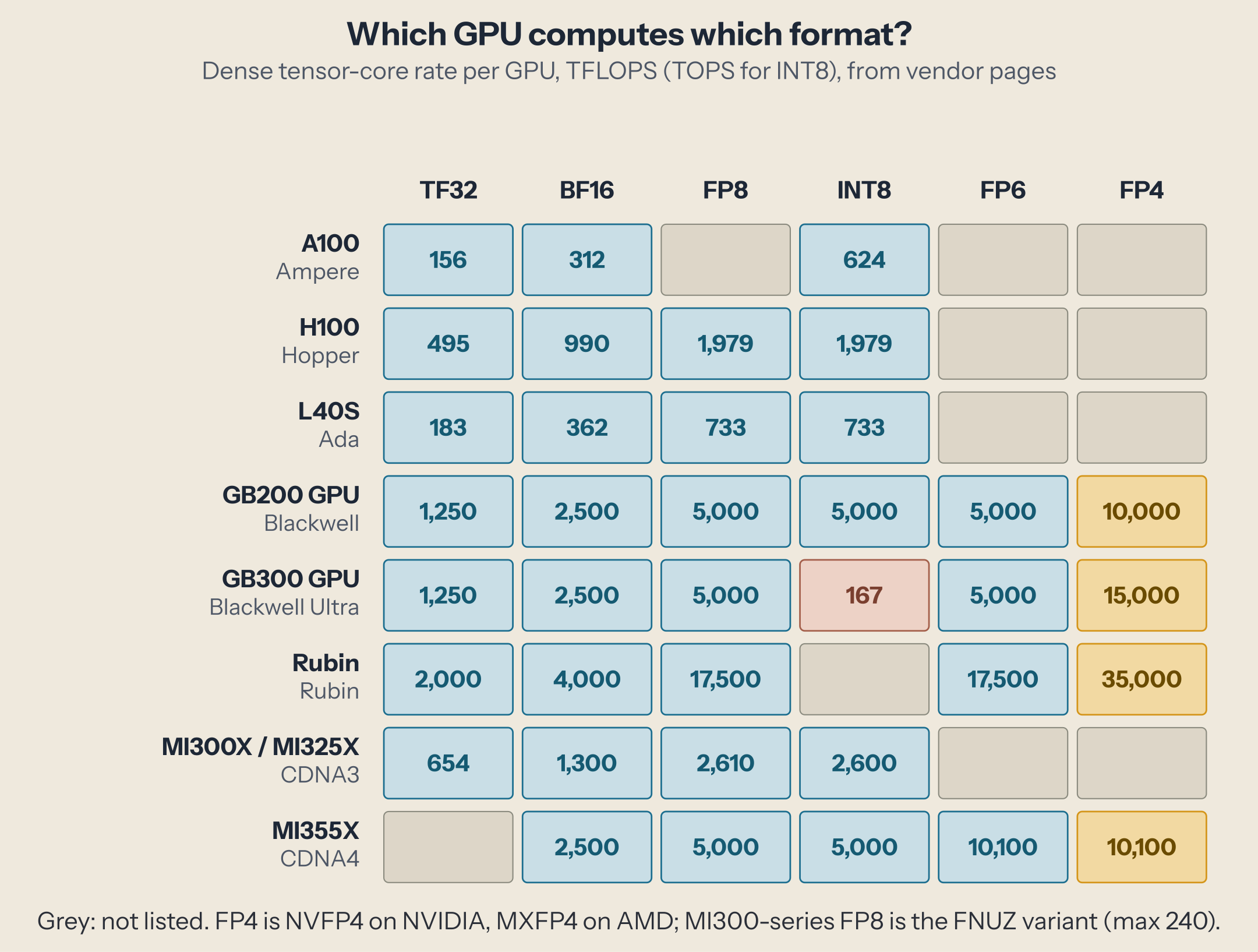
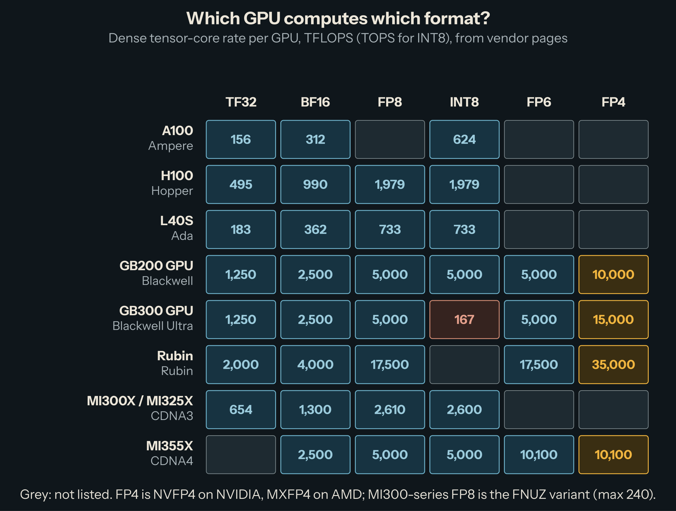
| GPU (architecture) | TF32 | BF16 | FP8 | INT8 | FP6 | FP4 |
|---|---|---|---|---|---|---|
| A100 (Ampere) | 156 | 312 | — | 624 | — | — |
| H100 (Hopper) | 495 | 990 | 1,979 | 1,979 | — | — |
| L40S (Ada) | 183 | 362 | 733 | 733 | — | — |
| GB200 GPU (Blackwell) | 1,250 | 2,500 | 5,000 | 5,000 | 5,000 | 10,000 |
| GB300 GPU (Blackwell Ultra) | 1,250 | 2,500 | 5,000 | 167 | 5,000 | 15,000 |
| Rubin | 2,000 | 4,000 | 17,500 | — | 17,500 | 35,000 |
| MI300X / MI325X (CDNA3) | 654 | 1,300 | 2,610 (FNUZ) | 2,600 | — | — |
| MI355X (CDNA4) | — | 2,500 | 5,000 | 5,000 | 10,100 (MXFP6) | 10,100 (MXFP4) |
Dense TFLOPS per GPU (TOPS for INT8); — means the format is not listed on the product page. Rubin's FP4 is NVIDIA's dense "NVFP4 training" figure; its "NVFP4 inference" figure is 50,000 with sparsity.
What the table shows
Halving the bits doubles the rate. On a GB200 GPU: BF16 2,500, FP8 5,000, FP4 10,000. The same doubling holds on H100 from BF16 to FP8, and on MI355X from FP8 to FP4. This is the hardware reason behind every format in this series: a smaller format is a faster format, if the GPU computes it natively.
INT8 is fading on NVIDIA. INT8 runs at the FP8 rate on Hopper, Ada, and Blackwell. On Blackwell Ultra, NVIDIA lists 24 POPS for a whole 72-GPU rack, about 167 TOPS per GPU, against 5,000 for FP8. Rubin's page has no INT8 line at all. Software follows: on a GB10 (Blackwell, compute capability 12.1), vLLM 0.31.0 refused to start an INT8 W8A8 checkpoint of Qwen3-8B with "Int8 not supported on SM121. Use FP8 quantization instead, or run on older arch (SM < 100)." If you are choosing an 8-bit format for weights and activations on NVIDIA hardware, FP8 is the one with a future; INT8 W8A8 checkpoints remain useful on older GPUs. AMD keeps INT8 at the FP8 rate on MI355X.
FP6 runs at the FP8 rate on NVIDIA, at the FP4 rate on AMD. NVIDIA lists "FP8/FP6" together; AMD lists MXFP6 at the MXFP4 rate (10.1 PFLOPS on MI355X). On MI355X, MXFP6 E2M3 is therefore as fast as MXFP4, and the microscaling piece measured it as accurate as FP8 (about 3% error on Qwen3-8B's weights, against 12% for MXFP4).
TF32 keeps growing on NVIDIA, from 156 on A100 to 2,000 on Rubin, while MI355X's page lists FP32 matrix throughput (157 TFLOPS) but no TF32 line.
Same name, different format
FP8 on MI300X and MI325X is not the OCP FP8 of the other GPUs. These GPUs use a variant called E4M3 FNUZ ("finite, no negative zero"), whose largest value is 240 instead of 448, and the same bits represent half the value. vLLM converts standard E4M3 checkpoints on the fly: it reinterprets the bits as FNUZ, doubles the scale to compensate, and replaces the one pattern that is zero in E4M3 but NaN in FNUZ. AMD's MI355X uses standard OCP FP8, as its product page states.
FP4 is two different formats. NVIDIA's GPUs list NVFP4; AMD's MI355X lists MXFP4. An NVFP4 checkpoint and an MXFP4 checkpoint are not interchangeable at the bit level, even though both store E2M1 values. NVIDIA's Blackwell page also says its tensor cores add "new community-defined microscaling formats", but the per-format MX rates are not on the product pages.
Without native support
When a GPU lacks a format, engines usually keep the compact weights in memory and convert them to 16 bits to compute. vLLM, for example, runs FP8 checkpoints on GPUs without FP8 hardware with its Marlin kernel, "weight-only FP8 quantization" for GPUs of compute capability 7.5 or higher, and has similar weight-only and emulation paths for NVFP4 (NVFP4 on Blackwell). You keep the memory savings, which is what limits decoding speed for small batches, but not the compute speed-up.
On the desk
Blackwell also reaches desktops. NVIDIA's DGX Spark (GB10) quotes "up to 1 PFLOP" of FP4 with 273 GB/s of memory bandwidth, and the RTX PRO 6000 Blackwell workstation card 4,000 FP4 TOPS with sparsity; neither page lists per-format rates. On a GB10, I measured a 4,096-cube matrix multiplication at 90.5 TFLOPS in BF16, 40.8 in TF32, and 17.4 in FP32 (TF32 and Accumulation).
What to take away
- Each generation adds a smaller format at about twice the rate: FP8 on Hopper and Ada, FP4 and FP6 on Blackwell and MI355X.
- Read datasheets as dense and per GPU; NVIDIA's headline figures are often sparse, and rack-scale figures cover 72 GPUs.
- INT8 is fading on NVIDIA (167 TOPS per GPU on Blackwell Ultra, not listed for Rubin); FP8 is the 8-bit format to bet on.
- "FP8" on MI300X/MI325X is FNUZ (max 240), and "FP4" is NVFP4 on NVIDIA, MXFP4 on AMD.
The last piece of the series looks at where low precision actually goes wrong in practice: rounding, overflow, and accumulation.
This post is part of the Number Formats for AI collection (8 of 9)

Inference engineering and AI in production — depth-first, no hype.
Inference Notes
Once a week: what changed in serving AI models, and what it means if you build, run or pay for them, in about five minutes.
Related Articles
DeepGEMM: The Matrix Multiplications Behind DeepSeek's Models
What DeepGEMM computes for DeepSeek's models: block-scaled FP8 and FP4 matrix multiplications, grouped GEMMs for MoE experts, and the fused Mega MoE kernel.
Your First CUDA Kernel, Compiled and Profiled
Write SAXPY in CUDA, compile it for a Blackwell GPU, check it, time it, and read what Nsight Systems and Nsight Compute say about it.
A GPU in One Picture: SMs, Warps, and Memory
The parts of a GPU that decide inference speed, from streaming multiprocessors to DRAM, with one real GPU's numbers and three measurements.